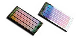
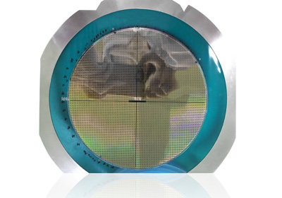
A wafer, also called a slice or substrate, is a thin slice of semiconductor material, such as a crystalline silicon, used in electronics for the fabrication of integrated circuits and in photovoltaics for conventional, wafer-based solar cells. The wafer serves as the substrate for microelectronic devices built in and over the wafer and undergoes many microfabrication process steps such as doping or ion implantation, etching, deposition of various materials, and photolithographic patterning. Finally the individual microcircuits are separated (dicing) and packaged.
We use cookies and similar technologies (also from third parties) to collect your deviceand browser information for a better understanding on how you use our online offerings.This enables us to optimize and personalize your experience with Ramsun and to provideyou with additional services and information based on your individual profile. Details areavailable in our privacy policy where you can also change your preferences on cookies atany time.