三年片免费观看大全第四集,东宫禁脔(H 调教),国产精品久久久久久久久动漫,成全电影大全在线观看国语高清

Contact us
Send E-MAIL
Home ? Product Center ? Flash ? MCP ? Nand MCP ? NAND MCP + LPDDR4 ?
Multi-chip package (NAND MCP) products are designed on the same substrate based on different storage technology processes. The superior chip stacking technology not only optimizes the design space of circuit boards, but also different storage technology products, including SLC NAND Flash and mobile DRAM. The power consumption DDR1, DDR2 or DDR4 is designed on a substrate. For applications to achieve faster startup time, longer battery life and higher reliability, the combination of mainstream NAND MCP products is 1Gb + 512Mb; 2Gb + 1Gb; 4Gb + 2Gb; 4Gb + 4Gb (NAND and low power DRAM).
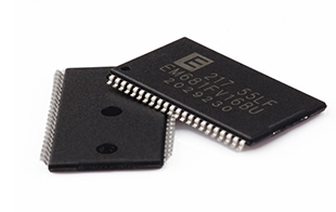
Jeju Semiconductor is one of the world largest SRAM solutions provider for mobile applications
Since Jeju Semiconductor made a debut to the SRAM (Static Random Access Memory) market in 2001 with 4M SRAM, Jeju Semiconductor continued implementing full lineup of low power SRAM products through 1M, 2M, 4M to 8M SRAM.
Tpye Part Number NAND(Density) NAND(Bus) NAND(Type) DRAM(Density) DRAM(Bus) DRAM(Type) ECC Speed Page Size Package Type Download
4Gb + 4Gb JSFCCE5QHAFGC-450B 4Gb x8 SLC 4Gb x16 LPDDR4x 4-bit 1600MHz 4K page 149B (8mm x 9.5mm) NULL
4Gb + 4Gb JSFCCE5QHABGC-405B 4Gb x8 SLC 4Gb x16 LPDDR4x 4-bit 1600MHz 2K page 149B (8mm x 9.5mm) NULL
4Gb + 2Gb JSFCBA5QH2FGA-405 4Gb x8 SLC 2Gb x16 LPDDR4x 4-bit 1866MHz 4K page 149B (8mm x 9.5mm) NULL
4Gb + 2Gb JSFCBA5QHAFGA-405A 4Gb x8 SLC 2Gb x16 LPDDR4x 4-bit 2133MHz 4K page 149B (8mm x 9.5mm) NULL
4Gb + 2Gb JSFCBA5QHABGA-405A 4Gb x8 SLC 2Gb x16 LPDDR4x 4-bit 2133MHz 2K page 149B (8mm x 9.5mm) NULL
4Gb + 4Gb JSFCCJ5QHABGC-405A 4Gb x8 SLC 4Gb x16 LPDDR4x 4-bit 2133MHz 2K page 149B (8mm x 9.5mm) NULL
4Gb + 2Gb JSFCBA5QHAFGA-405B 4Gb x8 SLC 2Gb x16 LPDDR4x 4-bit 1600MHz 4K page 149B (8mm x 9.5mm) NULL
4Gb + 4Gb JSFCCJ5QHABGC-405B 4Gb x8 SLC 4Gb x16 LPDDR4x 4-bit 1600MHz 2K page 149B (8mm x 9.5mm) NULL
4Gb + 4Gb JSFCCE5QHAFGC-450 4Gb x8 SLC 4Gb x16 LPDDR4x 4-bit 1866MHz 4K page 149B (8mm x 9.5mm) NULL
4Gb + 4Gb JSFCCE5QHABGC-405 4Gb x8 SLC 4Gb x16 LPDDR4x 4-bit 1866MHz 2K page 149B (8mm x 9.5mm) NULL
4Gb + 4Gb JSFCCJ5QHAFGC- 405 4Gb x8 SLC 4Gb x16 LPDDR4x 4-bit 1866MHz 4K page 149B (8mm x 9.5mm) NULL
4Gb + 4Gb JSFCCJ5QHABGC-405 4Gb x8 SLC 4Gb x16 LPDDR4x 4-bit 1866MHz 2K page 149B (8mm x 9.5mm) NULL
4Gb + 4Gb JSFCCA5QHAFGA-405 4Gb x8 SLC 4Gb x16 LPDDR4x 4-bit 1866MHz 4K page 149B (8mm x 9.5mm) NULL
4Gb + 4Gb JSFCCE5QHAFGC-450A 4Gb x8 SLC 4Gb x16 LPDDR4x 4-bit 2133MHz 4K page 149B (8mm x 9.5mm) NULL
4Gb + 4Gb JSFCCE5QHABGC-405A 4Gb x8 SLC 4Gb x16 LPDDR4x 4-bit 2133MHz 2K page 149B (8mm x 9.5mm) NULL
4Gb + 4Gb JSFCCJ5QHAFGC- 405A 4Gb x8 SLC 4Gb x16 LPDDR4x 4-bit 2133MHz 4K page 149B (8mm x 9.5mm) NULL
4Gb + 2Gb JSFCBA5QHABGA-405B 4Gb x8 SLC 2Gb x16 LPDDR4x 4-bit 1600MHz 2K page 149B (8mm x 9.5mm) NULL
4Gb + 2Gb JSFCBA5QH2FGA-405B 4Gb x8 SLC 2Gb x16 LPDDR4x 4-bit 1600MHz 4K page 149B (8mm x 9.5mm) NULL
4Gb + 2Gb JSFCBA5QHAFGA-405 4Gb x8 SLC 2Gb x16 LPDDR4x 4-bit 1866MHz 4K page 149B (8mm x 9.5mm) NULL
4Gb + 2Gb JSFCBA5QHABGA-405 4Gb x8 SLC 2Gb x16 LPDDR4x 4-bit 1866MHz 2K page 149B (8mm x 9.5mm) NULL
4Gb + 4Gb JSFCCJ5QHAFGC- 405B 4Gb x8 SLC 4Gb x16 LPDDR4x 4-bit 1600MHz 4K page 149B (8mm x 9.5mm) NULL
Open

      <menu id="qnkkk"></menu>
      <center id="qnkkk"></center>

      <pre id="qnkkk"><li id="qnkkk"><code id="qnkkk"></code></li></pre>
        <track id="qnkkk"><label id="qnkkk"><label id="qnkkk"></label></label></track>
        1. 主站蜘蛛池模板: 保定市| 喀喇| 澄城县| 项城市| 射洪县| 莎车县| 呼图壁县| 大城县| 阜新| 丹寨县| 焦作市| 育儿| 交口县| 宝丰县| 平安县| 苏州市| 湖北省| 清原| 贵定县| 手游| 固原市| 东海县| 博野县| 县级市| 开阳县| 西城区| 德格县| 同江市| 闸北区| 吉水县| 永兴县| 南岸区| 贵溪市| 宁城县| 延安市| 文安县| 汾西县| 萝北县| 绥中县| 商都县| 突泉县|